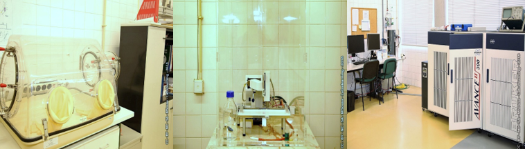
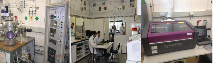
i3N integrates top facilities as required by high level research groups having as objective to be in forefront edge of research, technological development and innovation in the demanded areas of advanced micro/nano materials, nanotechnologies and nanosciences, and being responsible for boosting all known industry/applied research. This involves the use of high powerful computing tools; sophisticated labs for characterization and processing activities, such as clean rooms; use of sophisticated equipment, in some cases highly expensive, such as SEM/FIB or ultra high vacuum units to process materials and devices; use of raw materials, special gases and components, among others. All this requires running funds, not only to maintain the existing facilities, but also to purchase the consumables and to pay the assistance to match existing tools for a specific process or characterization required along an experience or project. To this, we must add also some seed money for the development of novel ideas, as well as to participate on missions.
For the large infrastructures, the required running funds are substantially larger, such as the funds required to maintain the existing 1000 m2 clean room facility, for the purpose of supporting research in the fields of microelectronics, electronic materials, nanotechnology, microfluidics, bioengineering, and devices and integrated circuits, requiring a low density particle environment.
Description: This lab is divided into three main areas. It has a common area equipped with a freeze dryer equipment, a furnace, an oven and general use equipment for sample preparation. It is equipped with a magnetic hyperthermia equipment intended to study the generated heat from magnetic nanoparticles. The third area of this lab is dedicated to fiber production composed with two electrospinning and one force-spinning set-up. This lab is also equipped with an Encapsulation unit to produce small polymer beads in a controllable manner.
For more information, here.
Description: The characterization lab is equipped with several equipments such as XRD, FTIR, Raman Microscopy, DSC-TG, UV-Vis_NIR spectrometer, luminescence spectrometer, spectroscopic ellipsometer, microplate reader and sun simulater.
For more information, here.
Description: The chemical lab is equipped with 3 microwaves synthesizers for performing a wide range of inorganic oxides nanoparticles such as ZnO, TiO2, IrO2 and Er2O3.
This lab has also 3 spin coaters to develop thin films used to produce different types of devices. In order to prepare the samples surfaces, the chemical lab is equipped with a UV ozone system integrated with an ozone elimination system.
The lab is equipped with all facilities for the synthesis and development of colloidal suspensions and nanoparticles generated in aqueous suspension.
For more information, here.
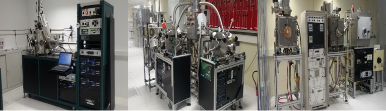
Description: The lab is equipped with a wide range of physical and chemical vapor deposition tools to fabricate a variety of thin film materials, such as metals, (transparent) conductors and semiconductors and insulators, with nm-thickness control. Most systems can accommodate up to 6” wafers. Tools include 5 sputtering, 2 plasma-enhanced chemical vapor deposition (PECVD), 4 evaporation and 1 CVD (parylene coater) systems. A rapid thermal processing (RTP) tool is also available for post-deposition treatments of thin films. A plasma-enhanced atomic layer deposition (PEALD) system with a glovebox for substrate loading/unloading in controlled environment will be installed in July 2019.
For more information, here.
Description: This lab is equipped with multiple manual probe stations and semiconductor parameter analyzers for I-V, C-V, pulsed-IV and time-dependent measurements (e.g. bias stress), from cryogenic temperatures to 300 °C. It also includes potentiostats for electrochemical studies, hall-effect systems and cryogenic chambers with electrometers for analysis of carrier transport in materials. The laboratory is also fully equipped to analyze dielectric materials and sensors, with lock-in amplifiers, spectroscopic impedance analyzers and an RLC bridge. Several oscilloscopes, power supplies, wave generators and high-power LEDs with several wavelengths are available for customizable measurement setups. Finally, in a separated area of the lab a last-generation X-ray and Ultraviolet Photoelectron Spectroscopy (XPS/UPS) tool is installed for chemical and electronic characterization of materials.
For more information, here.
Description:This lab has three distinct areas. The first one is equipped with one chemical lab with a working station and lab equipment for manipulation of different materials and ink development, it also has a screen stencil printer, fully automated for mass-manufacturing of printed devices, two office printers, adapted for different inks and devices, a centrifuge and a extruder. The second area is a yellow zone, for handling of UV-sensitive materials and inks. The third area is a production area, dedicated to paper electronics technology, for the production of low cost flexible devices, using different deposition methods, such as a flexoprinter, two piezoelectric inkjet printers, a multicoater with interchangeable heads (dip coating, spray coating, electrospinning and inkjet printing), a spray pyrolisis equipment for large-area manufacturing of devices, two different shear casting equipments, with heated and magnetic beds, a viscometer for measuring ink viscosities, a sonicator, with two interchangeable tips, for suspensions, particle dispersion, homogenization, etc. and a table-top vacuum packaging machine.
Fore more information, here.
Description: The liquid crystalline networks and liquid crystals laboratory is a multidisciplinary laboratory dedicated to research and development of bioinspired products, concepts and ideas. This laboratory has three distinct areas dedicated to the synthesis of liquid crystals and liquid crystal polymers mainly derived from cellulose derivatives, its processing to obtained films, networks and meshes and its optical and mechanical characterization.
In the synthesis area our laboratory is equipped with the appropriated glassware and small equipment as mantles, magnetic and mechanical stirrers, centrifuges, and also enables the synthesis of nanoparticles. To process the liquid crystalline material the laboratory is equipped with an electrospinning system, an automatic film applicator a spin coater and several ovens and furnaces. In the third area the laboratory has the means to characterize the produced materials by mechanical testing (1 to 10 cm scale samples), polarized optical microscopy and wettability measurements.
For more information, here.
Description: The NMR lab is a multidisciplinary lab that allow synthesis and characterization of soft materials. This lab has two main distinct areas, one for chemical synthesis and materials prepara-tion and another for characterization. The chemical area is equipped with typical appa-ratus such as a hotte, rotovapor, heating plates, glove box, oven, and all the necessary lab ware. The characterization area is equipped with a Bruker 300 MHz Solid State NMR spectrometer with an AVANCE III console, allowing the NMR characterization of solids and solutions using techniques such as Diffusion, rheo-NMR or Magnetic Res-onance Imaging (MRI). It is also equipped with a Langmuir–Blodgett apparatus that allows the production of highly organized thin film (typically monolayers) coatings of nanoparticles as well as the measurement of parameters such as concentration-dependence of surface tension. Another equipment available is an optical bench that allows to characterize the interaction of materials with a laser beam, namely by perform-ing electro-optical measurements. The lab is also equipped with a double beam UV-Vis spectrophotometer allowing the measurements of transmissions and absorbance of sam-ples as well as UV-Vis spectrometry.
For more information, here.
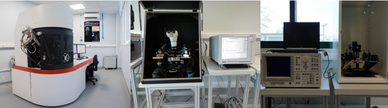
Description: This laboratory is equipped with a Scanning Electron Microscopy Focused Ion Beam (SEM-FIB) workstation, Atomic Force microscopy unit, confocal microscope and a tabletop microscope. It has also a contact angle instrument for automated video contact angle metrology and drop shape analysis, 2 profilometers that measure roughness and step height, optical microscope and optical stereo microscope.
For more information, here.
Description: The lab 2.20 in CEMOP is a dark room assigned to opto-electronic measurements, mainly dedicated to the characterization of photovoltaic devices.
The lab is equipped with three solar simulators and two spectral response (i.e. quantum efficiency) systems, as well as installed air extraction, air conditioning and compressed air flow.
For more information, here.
Description: This lab is dedicated to the processing of ceramic materials, glasses, metals and composites. This lab has distinct areas. It contains several electrical furnaces that are used in the production of metal and in different heat treatments. It contains mixing equipment, hydraulic pressing machines and several electrical furnaces (kilns and tubular furnaces up to a temperature of 1500ºC) that are used in the sintering of the ceramic powders, preparation of glasses by melting and in different heat treatments. It is equipped with one 3D printer for the development of prototypes and to support the ongoing projects.
For more information, here.
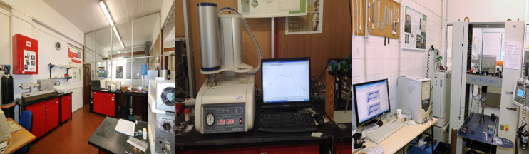
Rheometry Lab (Cenimat) Description: In this laboratory the flow behavior (in the linear and non-linear viscoelastic regimes) of different kind of fluids, polymeric (and biopolymeric) solutions and molten polymers and biopolymers, ceramic pastes, hydraulic lime grouts, bitumen, foods and cosmetics, etc., may be characterized.
Rheometry Lab (DCM) Description: In this laboratory the flow behavior (in the linear and non-linear viscoelastic regimes) of different kind of fluids, polymeric (and biopolymeric) solutions and molten polymers and biopolymers, ceramic pastes, hydraulic lime grouts, bitumen, foods and cosmetics, etc., may be characterized.
For more information, here.
Description: This lab is dedicated to the structural and compositional characterization of materials.
This lab has three distinct areas: X-ray diffraction area, SEM/EDS area and X-ray fluorescence area.
For more information, here.
Description: Photoelectron spectroscopy is a surface analysis tool for chemical and electronic characterization of materials. Its distinguishing feature is the possibility to measure chemical states. The information depth is 1-9 nm. The technique relies on the photoelectric effect. The photoexcitation energies typically range from ~20 eV (UPS) to ~1.5 keV (XPS). The photoelectrons are filtered regarding their kinetic energy by the analyser and counted by the detector. The lower the kinetic energy of the photoelectron, the more tightly it was bound to the nucleus, so the higher is its binding energy. Besides chemical information, also electrostatic potentials at surfaces and interfaces can be studied.
Equipments: X-ray and Ultraviolet Photoelectron Spectroscopy (XPS/UPS) Kratos Axis Supra
For more information, here.
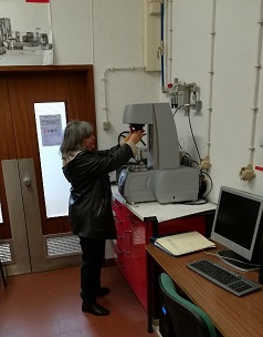
Description: This lab is dedicated to the Thermal, mechanical, thermomechanical and gragulometric characterization of materials.
The existing facilities are specific for powder technology and for processing of ceramic materials and glasses. It contains milling equipment and it also has a variety of characterization facilities such as a gas pycnometer for density measurement, particle size distribution analyzer by laser diffraction and thermal analysis equipment (DTA, TG, TMA and a dilatometer) that can be operated up to 1500ºC.
For more information, here.
Description: The thin film lab is a multidisciplinary lab that allow the development of new concepts and ideas.
This lab has three distinct areas. It is equipped with one chemical lab with a microwave synthesizer equipment to produce nanoparticles of different materials, a production area with two laser systems to cut, engrave and process different type of polymeric materials, several ovens and furnaces, a sputtering system and a thermal evaporator system to develop thin films. The third area is dedicated to lab-on-paper technology for the production of low cost biosensors and digital microfluidics and as also two 3D printer for the development of prototypes and to support the ongoing projects.
For more information, here.
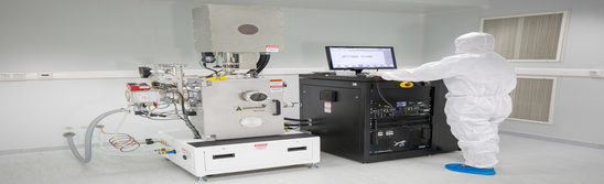
Description: The facility comprises 3 clean rooms, 2 ISO6 (class 1000) with 50 m² and 1 ISO7 (class 10 000) 80 m² and an access hall ISO7 with 60 m².
One of the ISO6 rooms is equipped with laser lithography system with optical alignment and assessment and a spin-coating and dip-coating systems.
Description: The Electrical and Magnetical Characterization Lab is equipped with two continuous flow cryostats working with N2 and He, two bath cryostats, two microfurnaces (Linkam THMS600 and Linkam TS1200), impedance analyzers and network analyzers (Agilent 8753D, Agilent 4294A, Modulab XM-Solartron Analytical – Ametek, AutoLab Spectro-electrochemical PGSTAT302N), a ferroelectric material characterization system (aixACCT-model TF2000), an electric polarization by Corona system (Brandenburg Alpha Series 807R High Voltage Power Supply and Brandenburg Gamma Series 828-20 High Voltage Power Supply), a Bruker EleXsys E500 electron paramagnetic resonance spectrometer, a computerized goniometer, a CFC- Cryogen Free Cryomagnet (Cryogenic) system with VSM Facility (Vibrating Sample Magnetometer) and AC Susceptibility. The system maximum magnetic field is 10 tesla and the sample temperature range is 1.6 K up to 300 K (700 K by coupling the VSM system oven), an XRD powder system (Aeris-Malvern Panalytical), and a DSC system (Hitachi-STA7300).
Description: Solar simulators, I-V and C-V of photovoltaic cells, Radiometric Platform, Organic Photovoltaics.
The materials and devices for energy lab has installed the required facilities for the preparation and basic characterization of fully operational thin film and organic solar cells based either in inorganic semiconductors such as chalcopyrites and kesterites or organic semiconductors.
For the materials preparation and processing, the lab has at its disposal a range of techniques such as RF- and DC-magnetron sputtering, e-beam evaporation, thermal evaporation incorporated into a glove box, rapid thermal processing furnace, tubular furnaces, high-power lasers, etc.
For the materials characterization the lab contains solar simulators, I-V and C-V measurement systems of photovoltaic cells, radiometric platform.
Description: The High-Performance Computing Lab at the University of Aveiro runs two x86-based clusters,
- ARGUS - with 1160 physical cores and 6.0 TB RAM and. The ARGUS cluster is connected by FDR56 Infiniband and has an Rpeak performance of 54 Tflop/s;
- BLAFIS - with 584 physical cores and 1.9 TB RAM. The BLAFIS cluster is connected by DDR Infiniband and has an Rpeak performance of 5 TFlop/s.
The facilities also include low-latency storage and backup units, and it is hosted at a datacenter in the Campus, providing uninterrupted room specs and technical assistance for this type of equipment.
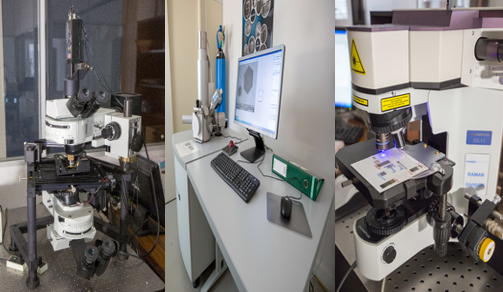
Description: SEM/EDX, AFM, SNOM, Raman.
SEM/EDX - The Scanning Electron Microscope (SEM) equipment relies on a TESCAN Vega 3 instrument. It is based on a thermal emission source (W filament), allowing beam energies within the 200 eV to 30 keV range.
It provides a 5 axis sample stage control (X,Y,Z, rotational, tilt), EDX analysis with 133 eV resolution (Bruker Nano X-Flash Detector 410-M) and ready-to-use Electron Beam Induced Current (EBIC) capability.
AFM/SNOM - Multiview 1000 Nanonics
a) Modes of Operation
Atomic Force Microscopy: Contact, Non-contact, intermittent contact.
Near-field Optical Microscopy: Transmission, reflection, collection, fluorescence.
Atomic Force Microscopy: Contact, Non-contact, intermittent contact.
Confocal Microscopy: Transmission, reflection, fluorescence.
b) Scanner: Piezo electric flat scanner (thickness 7 mm). Scan Range:70 µm Z-range, 70 µm XY-range (30 and 10 µm on request). Maximum Load: 75 g.
Step Size: < 1 nm for 70 µm scanner. Maximum Sample Size :16 mm diameter, custom mounts for larger samples can be provided.
c) Viewing/Detection Optics : Free optical access to the sample from top and bottom for optical observation of the sample (all conventional far-field modes of operation are available) and for detection of the NSOM signals with any optical microscope (upright, inverted, dual) or other optics.
d) Detectors and Lasers: Photomultiplier Tube (PMT), Avalanche Photodiode Detector (APD), InGaAs Detector for IR, CCD. A large variety of laser systems can be used (VIS, IR).
Near-field Microscopy optical resolution: From 50 nm upwards, depending on the aperture size of the NSOM probe used.
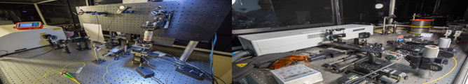
Description: Optical and electro-optical characterization of materials, quantum emission yield, colour coordinates, No Lab fs Laser radiance and luminance, Laser printing of Bragg gratings in optical fibers for sensors.
The Nanophotonics and Optoelectronics Laboratory is located at Aveiro University and its activities are mainly focused on optical modeling and simulation and on the development and application of advanced micro- and nano- optical fiber sensors in several fields, namely chemical, structural health monitoring and eHealth.
The existing infrastructure laboratory include a fs laser facility (1.0kHz repetition rate; 1.0mJ energy per pulse; vertical/horizontal polarization; 795nm ± (10 nm center wavelength; 22 ± 5ºC environment temperature) and a radiometric platform for measurements and analysis of optical performance as function of temperature.
The Nanophotonics and Optoelectronics Laboratory is equipped with a Femtosecond laser system, Q.switched UV laser system, Climatic Chamber, Radiometric platform and a Characterization kit of ultra-short laser pulses.
Laser:
• Quantronix, model Integra-C-1.0-F
• Centre wavelength 800 +/- 10 nm
• Pulse energy > 1.0 mJ
• Repetition rate 1 kHz
• Pulse width < 130 fs
• Pulse to pulse stability < 0.5% rms
• M2 factor < 1.3
Description: FTIR, absorption/transmission (VUV, UV, VIS, IR), photoluminescence (PL), PL excitation (PLE), time resolved PL (TRPL), lifetimes, excitation density/energy/temperature (4.5 – 900 K) dependent PL, electroluminescence (EL), photoconductivity (PC), Raman (laser lines: 325, 442, 532, 633 nm; polarization analysis; temperature LN2-600 C; imaging).
Description: The quality control and food safety laboratory is located at Madeira University and its activities are strongly focused on the development and application of novel advanced purpose-designed optical fiber sensors that can improve the quality control processes in food and beverages industries.
The existing infrastructure laboratory include a 10 x 200 L pilot scale unit; a HPLC with DAD, FD and RID; a GCMS with automatic HS- SPME; a LC-MS/MS; Spectrometer UV/Vis; Spectrometer NIR/MIR and a 7L Bioreactor.
Description: The Lab is fully equipped with ionization radiation sources, radiation detectors and medical imaging systems and all the needed equipment for detector development.
Radiation sources including a Radioisotope Laboratory and X-ray facility with 4 X-ray generators (60 kV/60 mA and a 50 kV/1 mA with continues operation; 30 kV solid state generator and; a dentistry generator with 70 kV).
Computed tomography (CT), Positron Emission Tomography (PET) and X-ray fluorescence imaging systems.
High and ultra-high vacuum systems, filling gas systems, flow mass controls and mass spectrometer.
NIM and VME electronic modules, amplifiers, high-voltage power supplies, logic, digitizers and multichannel analysers.
High performance digital oscilloscopes (e.g. 3.5 GHz, 2.5 GHz, 12 bits), picoammeters, pulse generators.
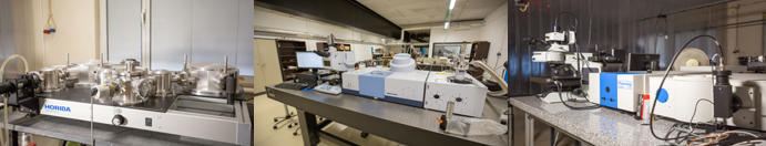
Description: DC and RF sputtering, e-beam deposition, thermal evaporation, spin-coating, spray-pyrolysis, sintering (furnace, sol-gel, combustion, microwave).
Laser processing lab is equipped with seven lasers systems that allow to produce functional interfaces and surface engineering, and the growth of single crystals, highly textured materials and nanoparticles. Chemical Vapor Deposition lab is equipped with two CVD reactors to the growth of carbon-based materials, particularly graphene electrodes for neural signals and GFETs biosensors.
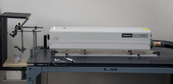
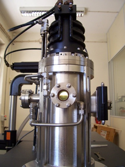
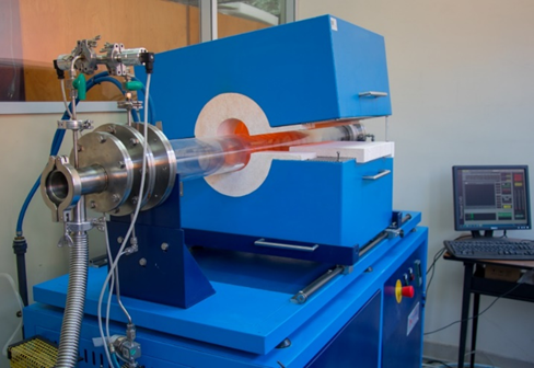
Laser Floating Zone (LFZ)
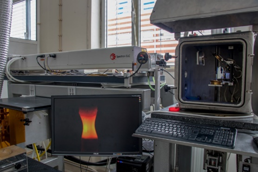
Description - LFZ system is mainly dedicated to the growth of single crystals and polycrystalline textured material (ZrO2, TiO2, ZnO, superconductors, thermoelectric, …), but also eutectic materials and metastable phases. The LFZ equipment includes a laser set-up; a growth chamber; monitoring system (laser parameters, pulling rate and rotation speed) assisted by real time image acquisition. The laser set-up comprises a continuous DC pumped 200 W CO2 laser (Spectron SLC, l = 10.6 μm) with a gaussian profile featuring a Reflaxicon optical arrangement. The growth chamber is sealed, enabling atmosphere-controlled processing.
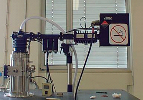
Pulsed Laser Ablation in Liquid (PLAL)
Description - Nanosecond (7 ns pulse width) Q-switched Nd:YAG laser emitting at 1064 nm wavelength and having a maximum pulse repetition rate of 10 Hz energizes. Under unfocused conditions, the laser beam has a spot diameter of 7 mm and a maximum pulse energy of 685 mJ. This system is equipped with a multiple nonlinear harmonic crystal generation unit allowing to obtain extra laser lines at 532 nm, 355 nm and 266 nm. PLAL system is mainly dedicated to the synthesis of nanoparticles (metallic (e.g. Au, Ag, Cu, …. ) or ceramic materials (e.g. ZrO2, phosphors, …). Also, materials dispersed in solutions can be exfoliated using PLAL technique (e.g. MoO3, ...).
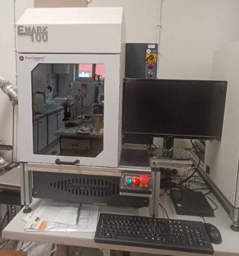
CO2 laser for surface modification/engraving/cutting
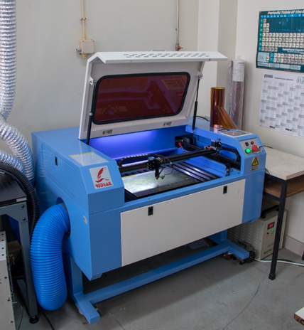
Description - CO2 laser emits a power of up to 50 W at the 10.6 µm wavelength in continuous wave regime.
The laser beam is directed through an optical system featuring an optical head attached to an automated XY gantry, achieving a well-focused scribing area of 30 x 50 cm2 at a maximum speed of 500 mm/s. Beam diameter at the focal point ~ 50 µm.
This system is mainly dedicated to surface modifications and cutting of different materials.
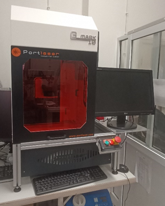
UV pulsed laser for surface modification/engraving/cutting
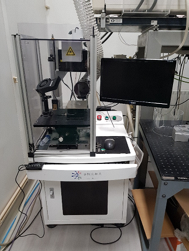
Description - A 5 W pulsed Laser, with a pulse frequency ranging from 10-150 kHz at a fixed wavelength of 355 nm. It is equipped with a galvanometric scanning head with a 16 mm F-θ Lens, allowing the controllable patterning at high speed in a 10x10 cm2 working area.
This system is mainly dedicated to surface modifications, development of functional interfaces and synthesis of new materials.
CO2 pulsed laser for surface modification/engraving/cutting
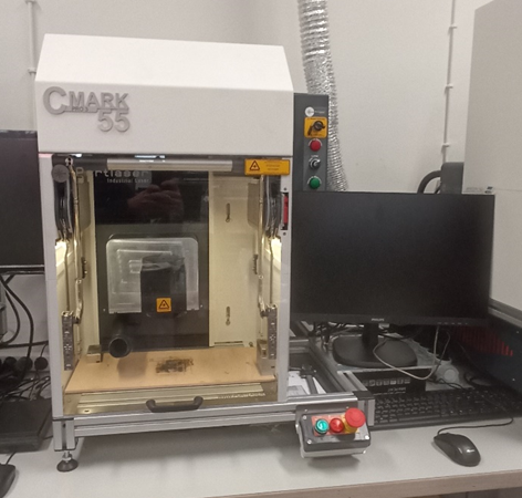
Description - Pulsed CO2 laser (?= 10.6 µm; 80 W), with a pulse frequency of 0.5 to 100 kHz, the laser beam is directed through a galvanometric head with an F-theta lens along the XY plane in a recording area of 100 x 100 mm2 at a maximum speed of 6000 mm/s.
This system is mainly dedicated to surface modifications, development of functional interfaces and synthesis of new materials.
Pulsed Fiber Laser for surface modification/engraving/cutting
Description - MOPA Pulsed Fiber Laser (λ = 1064 nm; 100 W), with a pulse frequency of 1 to 4000 kHz and pulse duration from 10 to 500 ns. The laser beam is directed through a galvanometric head with an F-theta lens along the XY plane in an area of recording of 110 x 110 mm2 at a maximum speed of 6000 mm/s.
This system is mainly dedicated to surface modifications, development of functional interfaces and formation of new materials.
Pulsed Green Laser for surface modification/engraving/cutting
Description - Nanosecond pulsed green laser (λ = 532 nm; 10 W), with a single-pulse pulse frequency up to 150 kHz (10 ns duration). The laser beam is directed through a galvanometric head with an F-theta lens along of the XY plane in a recording area of 100 x 100 mm2 at a maximum speed of 6000 mm/s. This system is mainly dedicated to surface modifications, development of functional interfaces and formation of new materials.
Picosencond UV laser for surface modification/engraving /cutting
Description - A 10 W 10ps UV (355 nm) MOPA laser with two possible outputs: A 3D galvo head system that allows to create 3D designs on surfaces or inside transparent materials, and a direct output to be connected to microscope lenses, allowing high resolution micropatterning. It works on different types of materials to promote micro and nanometric changes with different topographies and therefore different surface properties.
This system is mainly dedicated to surface modifications, development of functional interfaces and synthesis of new materials.
Microwave Plasma Chemical Vapour Deposition (MPCVD)
Description - A high-power microwave magnetron is coupled trough a rectangular profile waveguide and an antenna to a cylindrical growth chamber.
MPCVD with 6 kW microwave max. power and is mainly dedicated to the synthesis of carbon allotropes (graphene, carbon nanotubes (CNTs) and diamond films).
Thermal Chemical Vapor Deposition (TCVD)
Description - TCVD reactor is able for reaching temperatures of up to 1200°C through resistive heating. It is composed of two coaxial quartz tubes (diameter: 75 mm inner tube and 95 mm outer tube; length: 1400 mm inner tube and 1500 outer tube), allowing deposition either between the tubes or in the inner one.
The system is equipped with a gas supply of argon, hydrogen and methane, and is capable of growing graphene at either atmospheric or low pressure, with the latter achievable using a roots-type dry pump.
Profilometer
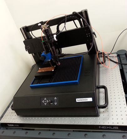
Description - Profilometer using chromatic dispersion technology. It allows to extract surface profiles (textures and topographies) with a lateral resolution of up to 1.7 um in large working area (150 x 200 mm2) and with a capture depth of up to 3 mm (which can be increased by multiple passes).
Potentiostat/Galvanostat
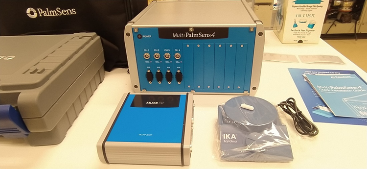
Description - Four-channel device for impedance spectroscopy (100 kHz – 10 µHz), Mott-Schottky analysis and several variants of voltammetry, amperometry, potentiometry and coulorimetry. Bi-potentiostat (for e.g. ion-sensitive and bioFET testing) and iR drop correction capabilities. It allows very sensitive measurements (5 fA resolution on the 100 pA range), adequate for micro/nanosensors and other small current magnitude applications. Channels can be synchronized and each channel can be extended by the multiplexer to allow 8 automated series measurements.
Potentiostat/Galvanostat
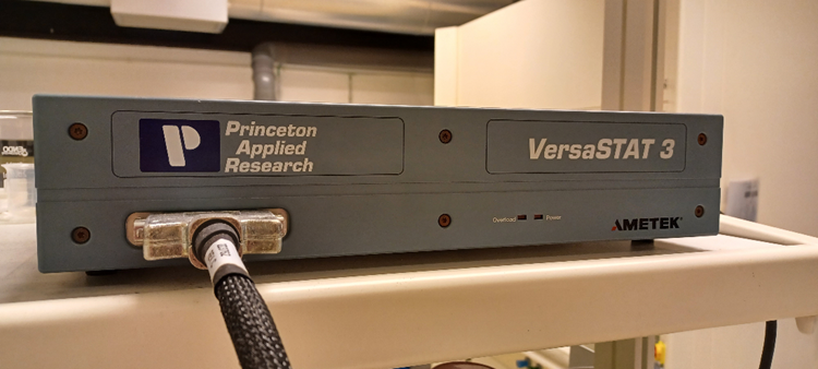
Description - Single channel device for impedance spectroscopy (1 MHz – 10 µHz) Mott-Schottky analysis and several variants of voltammetry, amperometry, potentiometry and coulorimetry. IR drop correction capability. The +/- 12 V potential range and 650 mA max current allows for testing electrode and electrolyte materials for most electrochemical applications, including sensors, catalysis and bulk electrolysis, as well as electrochromic devices and energy storage devices such as small batteries and coin cells.
Spectrometer VIS-NIR
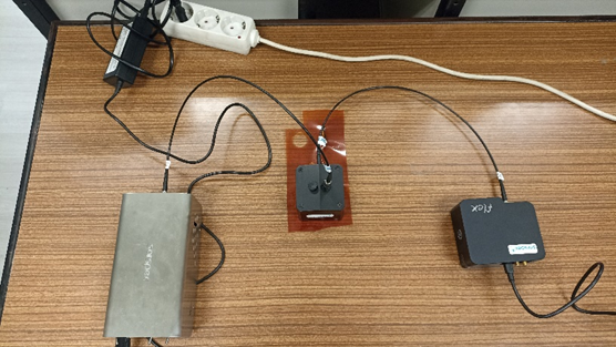
Description - Flex Spec spectrometer with a wavelength range of 360 to 1100 nm, the optical resolution is 0.6 nm with a 10 μm slits. The system is equiped with a Y-Probe, in which is possible to characterize the diffuse and specular reflection.
Also, with an integrating sphere the signal to noise racio is increased making it possible to characterize low reflective samples.
Optical power meter with fan cooled S322C thermal power sensor head
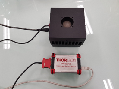
Description - Power and energy meter interface with USB operation with
fan cooled S322C thermal power sensor head
Wavelength Range: 250 nm - 11 µm
Optical Power Range: 100 mW - 200 W
Active Detector Area: Ø25 mm
Max Optical Power Density: 4 kW/cm²
Resolution: 5 mW
Raman spectrometers (532 and 785 nm)
Description - Micro-Raman system with two laser lines 532 and 785 nm. This integrated micro-Raman system with optical fiber coupling is coupled to a microscope and allows to quickly obtain structural information from various types of samples.
Van der Pauw system for sheet resistivity
Description - A probe fixture connected to a multiplexer interface and a Keysight B2902A to perform 4-proble sheet resistance measurements.
FLIR A310 Thermal Camera
Description - Thermal Camera with a 320 x 240 resolution able to detect temperature differences down to 50 mK, with a field-of-view of 25°x 18.8°.